As Intel attracts billions in investment, onboarding external customers to 18A will inform the future of cutting-edge semiconductor fabrication in the United States
During the recent Intel Technology Tour in Arizona, the company shared details of its forthcoming client and server SoCs, both of which are built on 18A, Intel’s latest process node. We’ll get into the details of the Intel Core Ultra series 3 (Panther Lake) and Intel Xeon 6+ (Clearwater Forest) but the key point here is less about product announcements, and more so about that these latest products are being manufactured using the most advanced process in the world, and that capability is located in the United States.
While the bulk of the Intel Technology Tour was dedicated to deep dives into the features and capabilities of Panther Lake and Clearwater Forest, as well as a look at edge AI use cases that can be delivered locally with on-device processing, the introductory keynote talks had a clear theme.
Listing off benefits Intel Foundry is delivering to the products side of Intel — RibbonFET, PowerVia, advanced packaging, and logic scaling and stacking — Chief Technology and AI Officer Sachin Katti said, “18A is the foundation for our future and we are fully focused on scaling it.”
Kevin O’Buckley, SVP and GM of Foundry Services, highlighted Fab 52, the latest addition to the company’s Ocotillo campus. “I’m going to be a little repetitive with you on one point:…We’re extremely proud to be bringing to market the world’s most advanced semiconductor technology available today in production in our 18A node. It’s built on the back of 57-plus years of investment by us at Intel in development and manufacturing here in the U.S. We’re very proud for the part that we’re playing in strengthening a resilient supply chain for our entire industry — something not just U.S. customers are asking for; something that’s critical for all customers globally.”

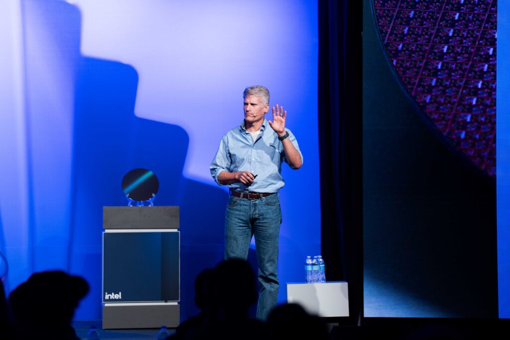
Auth discussing 18A. Image courtesy of Intel.
Next up, VP and Director of Advanced Technology Programs and Services Chris Auth took the stage. He shared details on RibbonFET, a gate-all-around transistor tech, and backside power delivery advancement PowerVia. He said production on the 18A node is ramping in factories in Arizona and Oregon.
“The key point here,” Auth continued, “is that these are the most advanced semiconductor facilities not only in the U.S. but in the world. Let me make sure you get that one: these are the most advanced semiconductor facilities in the world…There’s a narrative that we don’t do advanced semiconductor manufacturing in the United States, but here we are doing it in two states in the U.S.” He said volume production on 18A “is going to launch a decade of enhancement and improvement” of RibbonFET and PowerVia. “And this really enables the chips of tomorrow and getting to that 1 trillion transistor laptop.”
Those of us in the storytelling business call this an escalating narrative. Katti emphasized scaling 18A as fundamental to Intel’s future outlook. O’Buckley framed 18A as important to Intel, important to the external customers it’s trying to onboard and important for global semiconductor supply chain resiliency. Auth dispensed with any subtext, acknowledging the narrative around Taiwan’s pole position in semiconductor fabrication technology, and asserting Intel’s (and by proxy the United States’) capability advantage.
Here’s what I think is a bit of interesting context and scene-setting. Intel hosted the event at the Sheraton Grand Wild Horse Pass, a resort that sits on land owned by the Gila River Indian Community and that was developed with extensive input from community elders. This resort is an incredibly tasteful immersion into the local culture, from on-site food and beverage offerings and the art and textiles in common areas and guest rooms to an interpretive trail and a local hiring preference. This is my observation — and I feel qualified to make it based on the volume of travel I do and that my wife is a career hospitality professional — but that combination of pride in place and staffing a place with people proud of it translates into a high-touch service experience that was very noticeable — shout out to Alex at the lobby bar; a real pro.

The Sheraton Grand Wild Horse Pass in Chandler, Arizona.
Across from Intel’s Ocotillo campus in Chandler, Arizona, is a bit of lovely farmland also owned by the Gila River Indian Community. Inside Fab 52 and other Intel fabrication facilities are machines and input materials and people from all over the world. All that to say, while the point (and importance) of the U.S. being a leader in advanced semiconductor manufacturing wasn’t wasted on me, the idea of sovereignty as a simple concept — when it absolutely is not — and of American exceptionalism as a function of decades of globalization, was also not wasted on me. But I digress…
The culmination of 5N4Y — a new transistor architecture, a new interconnect approach
The launch of products built on 18A is the culmination of years of work from Intel, including a new transistor architecture, a new approach to interconnect and myriad chiplet packaging advancements. 18A is also the conclusion of the five nodes in four years (5N4Y) strategy announced in July 2021 — this was essentially Gelsinger’s turnaround strategy. The five nodes, key features and notable products are:
- Intel 7, a 10-nanometer process marked by the Enhanced SuperFin (ESF) transistor architecture, and used for Alder Lake and Sapphire Rapids.
- Intel 4, a 7-nanometer process that introduced Extreme Ultraviolet (EUV) lithography, and was used for Meteor Lake and Granite Rapids. This process also marked the move to chiplet packaging.
- Intel 3, a 3-nanometer process that, compared to its predecessor, improved performance per watt by 18%, and was productized as Xeon 6.
- Intel 20A marked a switch from nanometer-based measurements to angstrom-based measurements; there are 10 angstroms in one nanometer. While 20A never made it into full-on production — Arrow Lake was fabricated by a third party and packaged by Intel — it “directly informed the first commercial implementation” of RibbonFET and PowerVia in 18A.
Back to Auth: “The heart of any semiconductor chip is the transistor and the interconnects that not only connect them together but to the outside world…Intel 18A has two of the most advanced features we’ve ever produced” — RibbonFET and PowerVia. “The combination of these two enable both area scaling and power efficiency…and it’s developed and manufactured here in the U.S.”
Around a decade ago, Intel introduced the FinFET transistor architecture which replaced 40 years of planar technology with a 3D technology where fins of silicon enabled increased density, albeit with a weak spot at the bottom because the gate couldn’t completely wrap around the transistor. “This is where RibbonFET shines,” Auth said. “There’s no weak points.” He described sheets of silicon layered on top of one another completely wrapped by the gate. “The RibbonFET transistor enables us to continue to scale the transistor.”
Before getting into PowerVia, Auth reflected on six decades of integrated circuits as marked by interconnects (power and signal) always formed on the front side of a wafer. Power lines, as the name suggests, bring power from the package to the transistor; signal lines let the transistors talk to each other. Power lines benefit from large lines with little resistance; signal lines want to spread out to minimize interference. “What we’ve done with PowerVia is we’ve taken those power lines, we’ve moved them from the frontside and put them on the backside of the wafer…We now have plenty of space to make big, fat power lines…and now, on the frontside, that opens up space. We can now allow the signal lines to spread out a little bit more.”
The result here is a 10% higher transistor density and reduction in power loss between the package and the transistors. Auth addressed the notion that backside power delivery would drive up costs: he said Intel didn’t slap a frontside process onto the backside of the wafer, rather optimized the process for backside power from the start; this reduced process cost and the number of steps compared to Intel 3. And, “Intel’s the only one who’s doing this in manufacturing today.”
Intel executives also emphasized the company’s advanced packaging and stacking technologies. For the casual reader, this is the process wherein different discrete chiplets — CPUs, GPUs, NPUs, memory, etc… — are put together into a single system. For Panther Lake, Intel utilized its Foveros advanced packaging technology, specifically Foveros-S 2.5D. The key benefits here are latency reduction delivered by minimizing the distance between components; optimal space utilization because components can be stacked rather than spread horizontally; and the potential for manufacturing cost reduction by using smaller, specialized dies on advanced nodes while reusing proven IP blocks on mature nodes to drive yield. Another relevant piece of the very complex puzzle is EMIB, Embedded Multi-die Interconnect Bridge, which relates to both Auth’s earlier comments on interconnects as well as complements Foveros
in terms of driving performance and functionality. More on Foveros here, and more on EMIB here.
Panther Lake features up to 16 performance (P) cores and efficient (E) cores; the new CPUs are 50% faster than the previous generation. The Arc GPU has up to 12 Xe cores which deliver 50% faster graphics performance than its predecessor. The major emphasis, which we’ll expand on in subsequent writing, was around leveraging Panther Lake’s in-built 180 TOPS for edge AI. Because fairly intensive processing of AI workloads can be conducted on-device, this brings numerous benefits around latency, security, cost and other factors, while also opening up applications for everything from retail and robotics to healthcare and traffic management. Expect devices featuring Panther Lake early next year, perhaps at everyone’s favorite consumer electronics show.
Clearwater Forest, which Intel characterized as “tailored for hyperscale data centers, cloud providers and telcos,” features up to 288 E-cores and brings improvements in density, throughput and power efficiency. The point here is scalable, power-efficient AI computing. To put this into real world context, consider a hypothetical telco data center running Intel’s second-gen Xeon chips on 1,400 servers across 70 racks. If that operator were to transition to Xeon 6+, they could do more with less — significantly less; a comparable setup would only take 180 servers in 20 racks. The move to Clearwater Forest would also bring about a 750-watt reduction in power draw and a 3.5x performance gain. With regard to packaging, Xeon 6+ will use Foveros Direct 3D, a first in high-volume manufacturing.
Under new CEO Lip-Bu Tan, Intel has made significant adjustments to its employee-base and global manufacturing investments. On a second quarter earnings call, Tan said, “Unfortunately, the capacity investment we made over the last several years were well ahead of demand and were unwise and excessive…Going forward, we will grow our capacity based solely on the volume commitments and deploy capex lockstep with tangible milestones, and not before.”
So while the company brings to market its own products built on 18A, and looks for “volume commitments” from external foundry customers, what does that mean for 14A, the next process node, and the longer-term outlook for developing leading-edge semiconductor fabrication capacity in the U.S.?
In a 10-Q filed on July 24, Intel told the SEC, that it will continue to develop 18A-P, a “derivative node…designed for future Intel products and external customers…We are focused on the continued development of Intel 14A…and on securing a significant external customer for such node. However, if we are unable to secure a significant external customer and meet important customer milestones for Intel 14A, we face the prospect that it will not be economical to develop and manufacture Intel 14A and successor leading-edge nodes on a go-forward basis. In such event, we may pause or discontinue our pursuit of Intel 14A and successor nodes and various of our manufacturing expansion projects.”
Four weeks, $15.9 billion in new investment
Intel has had an interesting and impactful 57 years but, as the company looks to reinvent itself for the AI era and attract non-Intel customers to its fabrication business, the company has had a particularly eventful past two months. I think it’s safe to call it an historic inflection point, or series of inflection points, spanning the technical, the financial and the organizational.
On Aug. 18, Japanese powerhouse SoftBank announced a definitive securities purchase agreement that saw it buy $2 billion of Intel’s common stock. SoftBank Founder and CEO Masayoshi Son said in a statement: “Semiconductors are the foundation of every industry. For more than 50 years, Intel has been a trusted leader in innovation. This strategic investment reflects our belief that advanced semiconductor manufacturing and supply will further expand in the United States, with Intel playing a critical role.”
Four days later, on Aug. 22, the Trump Administration agreed to invest $8.9 billion in Intel common stock. That money came from unawarded CHIPS and Science Act grant funding ($5.7 billion) and from the Secure Enclave program ($3.2 billion); the government has also dispersed $2.2 billion in CHIPS and Science Act grants to Intel. Tan, who replaced Pat Gelsinger late last year, said in a statement: “As the only semiconductor company that does leading-edge logic R&D and manufacturing in the U.S., Intel is deeply committed to ensuring the world’s most advanced technologies are American made. President Trump’s focus on U.S. chip manufacturing is driving historic investments in a vital industry that is integral to the country’s economic and national security.”
On Sept. 8, Tan made public significant changes to Intel’s leadership. Formerly of NXP, Qualcomm and Arm, among others, Kevork Kechichian joined as EVP and GM of the Data Center Group to oversee the cloud and enterprise data center business which also includes the Xeon line. Intel veteran Jim Johnson was named SVP and GM of the Client Computing Group, looking after the PC and edge businesses. Srini Iyengar, who joined Intel from Cadence Design Systems in June, was put in charge of the new Central Engineering Group to “lead horizontal engineering functions and build a new custom silicon business to serve a broad range of external customers.” Intel Foundry EVP and Chief Technology and Operations Officer Naga Chandrasekaran, formerly of Micron, took on an expanded role to include Intel Foundry Services; the idea was to “create a more integrated structure spanning technology development, manufacturing and go-to-market to better serve customers.”
Then, on Sept. 18, Intel and NVIDIA announced a new product development partnership, as well as that NVIDIA would invest $5 billion in Intel common stock. On the product side, the two companies are working to connect Intel and NVIDIA architectures using the former’s NVLink interconnect solution. For the data center, Intel is building customized x86 CPUs that NVIDIA will integrate into its AI infrastructure platforms. For client, Intel will integrate NVIDIA RTX GPU chiplets into its x86 SoCs.
Inside Intel’s Fab 52 — the machinery that’s building our future
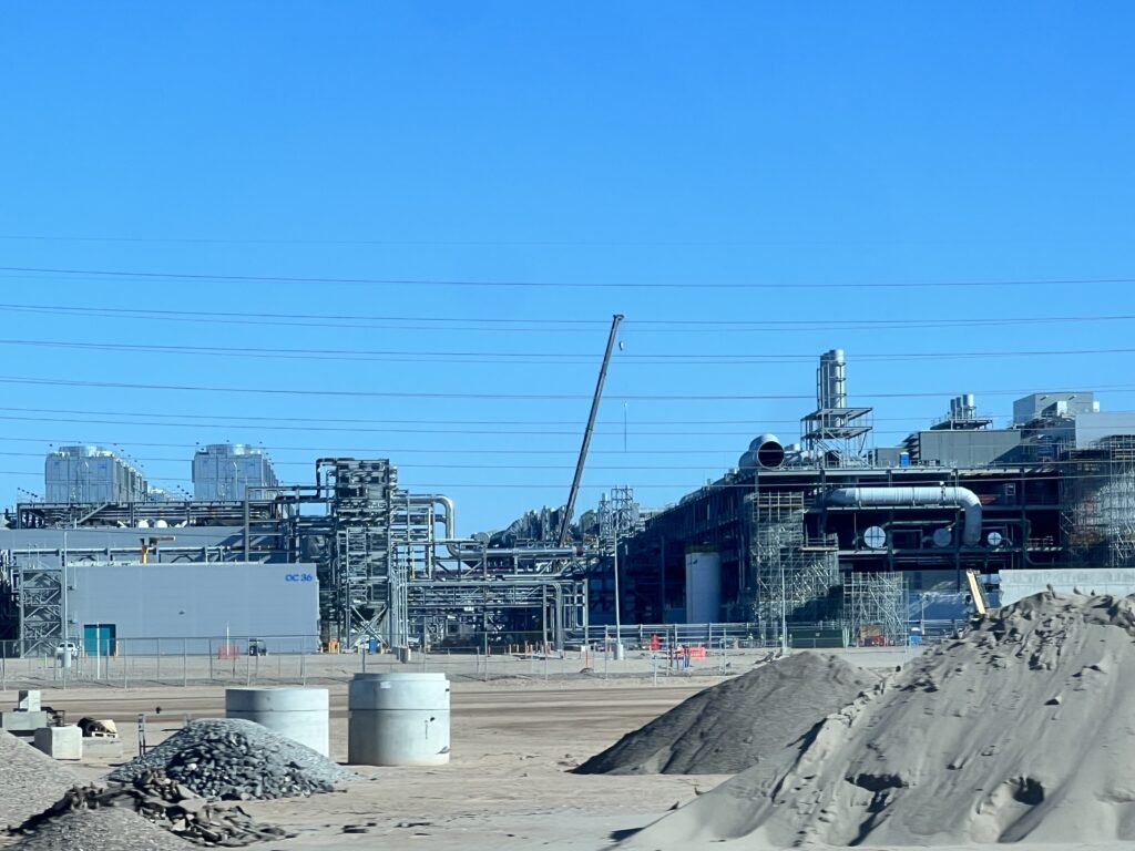
The crescendo of the Intel Technology Tour was a tour of fabs 42 and 52 at the Ocotillo campus. Construction on Fab 52 started in 2021 and it’s now fully operational and set to reach “high-volume production” later this year. Here are a few facts about the Fab 52 construction process courtesy of Intel: more than 1 million meters of soil and rock — the equivalent of 400 Olympic-size swimming pools — were excavated; around 600,000 cubic meters of concrete was poured; 75,000 tons of steel, double what was used to build the Burj Khalifa in Dubai, was used for reinforcement; and 35,000 tons of structural steel, five-times the weight of the Eiffel Tower, was erected. And there’s also room on the site for a Fab 62…

Anyway, those facts and figures are interesting but, relative to walking through the fabs — actually seeing the whole system at work — it’s kind of like trying to describe to someone what sunset over the Grand Canyon feels like. It’s an abstract, personal thing, which is a dissonant statement because it’s also a very tangible, physical process.
After receiving a security briefing and donning a bunny suit in a gowning room, we walked through Fab 42 and into Fab 52. The level of automation is remarkable. A ceiling-mounted automated materials handling system whizzes front-opening unified pods containing silicon wafers from machine to machine. Rows and rows of enormous implements are labelled with an animal/numerical system meant to ensure engineers work on the right of the near-identical looking tools. The ambient noise of the air recirculation system is quite loud, and the yellow light (necessary so as to not interfere with the delicate equipment) gives the whole thing a bit of an alien texture.
All that to say, I found my time in the fabs to be quite overwhelming, stimulating and remarkable, really. It’s not readily quantifiable but I think this is maybe the most complex, precise thing that humans have figured out how to do. The regard for semiconductor fabrication as a strategic geopolitical asset is correct, as is the investment in diversification of the semiconductor supply chain; given America’s pedigree in high-tech industry, there’s a clear logic in building out more capacity here. Nationalistic narratives generally turn me off but this one does not.
My three-year-old son is constantly playing with pulleys, screwdrivers, wire and other things that he generally refers to as “machinery;” what that means to him isn’t exactly clear to me. What is clear to me though is that those fabs in the Arizona desert contain the machinery building my future, his future and our collective future. Whether it’s right or wrong, something about that machinery being in the United States gives me a sense of peace and pride.

